quasivoid
SBM-20 based geiger counter (first attempt)
A few months ago, I impulse bought an SBM-20 geiger-mueller tube on ebay because I thought NOS Soviet stuff was swag. I had not done any research. It quickly became apparent that I would have to design a 400V power supply to make it work. I had barely started learning about electronics by this point, and I ended up getting thrown into the deep end here. Especially since I established a particular goal of not using any pre-existing design whatsoever unless I understood it completely enough that I could have designed it myself.
quick aside: Nuts and Volts magazine style power supplies
https://www.nutsvolts.com/magazine/article/pocket-geiger-unit
When you look into doing this, common recommendation points to this circuit. Many kits also use this design. While I was studying it, I came to dislike it. There isn’t any regulation, which is fine in itself, and the original author makes a good case for it:
In DC-DC converter handbooks, you’ll find the flyback converter described as a constant-power device whose output voltage, unless stabilized, varies greatly with the load resistance. Each switching cycle delivers the power stored in an inductor to the load. Either the peak inductor current, or the switching frequency, is adjusted to maintain a constant voltage. What is less well known is that when the load current is low enough, a flyback converter behaves as a constant voltage source. It converts the peak inductor current to output voltage in a ratio that depends only on the inductor and the capacitance associated with it. This transimpedance ratio is the square root of L/C, and with practical components, can exceed 20 kV per amp. A 450 V output, for example, requires a peak inductor current around 20 mA. You can generate a stable high voltage with no transformers or voltage multipliers, just an inductor, a switch transistor, a rectifier and a reservoir capacitor.
However, while analyzing the circuit, I had an incredibly difficult time figuring out what capacitance he was talking about. Eventually, I realized that this depends on the parasitic capacitance of the inductor. To me, in my computer science background, this struck me like relying on undefined behavior, so I started down the road of more traditional SMPS topologies. Besides, I was already fascinated by SMPS, and wanted an excuse to implement a “proper” one.
In retrospect, I dont think the parasitic capacitance is really undefined. Looking at the datasheet of the inductor I chose now, the self resonant frequency is declared, from which the capacitance may be calculated. Anyways.
a switch mode power supply!
Okay, the other thing you see a lot when going down this route is people naiively suggesting that a flyback topology is the correct way to do this, because of the huge voltage gain involved (from battery power to 400V!). This suggestion seems to be made by people that dont realize that geiger-mueller tubes hardly use any power whatsoever, with current draw on the order of microamps. In fact, in absence of a radiation event, it is an open circuit (its a capacitor!).
I found it very difficult to design an effective flyback supply simply on the basis of almost all of the power being consumed in the resistive feedback circuit. Enter, Analog Devices CN-0536:
https://www.analog.com/media/en/reference-design-documentation/reference-designs/cn0536.pdf
This was extremely eye opening when I came across it. I had already implemented little supplies using a 555 and comparator successfully, it was just the high voltage thing that was stumping me. By using a voltage multiplier, you can take feedback from a lower voltage, so less resistance is needed to make a low-current feedback circuit. Regulation is looser but it doesn’t need to be a tight, geiger-mueller tubes are very tolerant of huge voltage ripple.
Their design parameters basically don’t apply to me at all. I did not make a micropower design. I used an LM311 and a TLC555. Thats not micropower. I cut out two stages and took feedback at a slightly higher voltage, and used a far lower impedance feedback network. Regardless, this approach is what got me over the finish line, as questionable as it is.
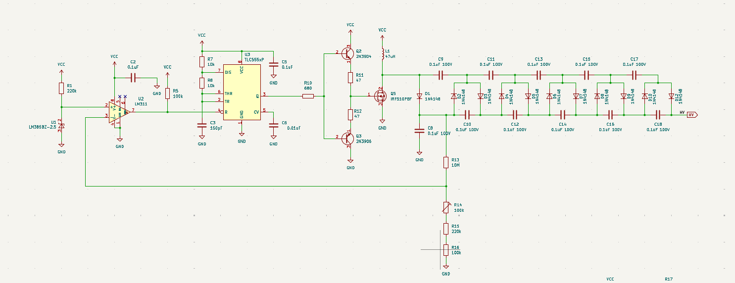
Error in the schematic. I realized last minute that there should be a large bulk decoupling capacitor right next to L1. I put this in a silly part of the schematic which is not captured in the screenshot (in the battery section). Anyways.
Also of note is the BJT push-pull circuit made from Q2 and Q3. This is so that Q5s gate may be charged and discharged in a timely manner without making too great demands from U3.
detector
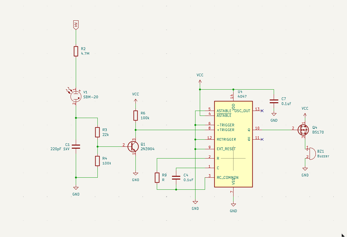
The first part of the detector is pretty much taken wholesale from MightyOhms geiger counter design, because I couldn’t come up with anything better. The tube is charged via its anode resistor to 400V. When a particle passes through, its charge gets dumped into C1, level-shifting the voltage down to approximately 7.8V. C1 discharges through R3 into Q1s base-emitter junction until it drops low enough that Q1 stops conducting, when it will continue to discharge through R3+R4.
Q1 is retained for the purpose of protecting U4, a CD4047, from high voltage transients on the input.
4047 converts the very short (14-ish microsecond) pulse to a more audible … some number of milliseconds pulse, as defined by R9 and C4. I left R9 undefined and calculated what I wanted it to be during assembly. I don’t remember what I selected. Anyways, point is, it makes an audible pulse.
A very silly error: Q4 should be on the low side of BZ1, not the high side! I hadn’t fully internalized MOSFET behavior when I designed that part. It -works-, at least, but probably not as it should…
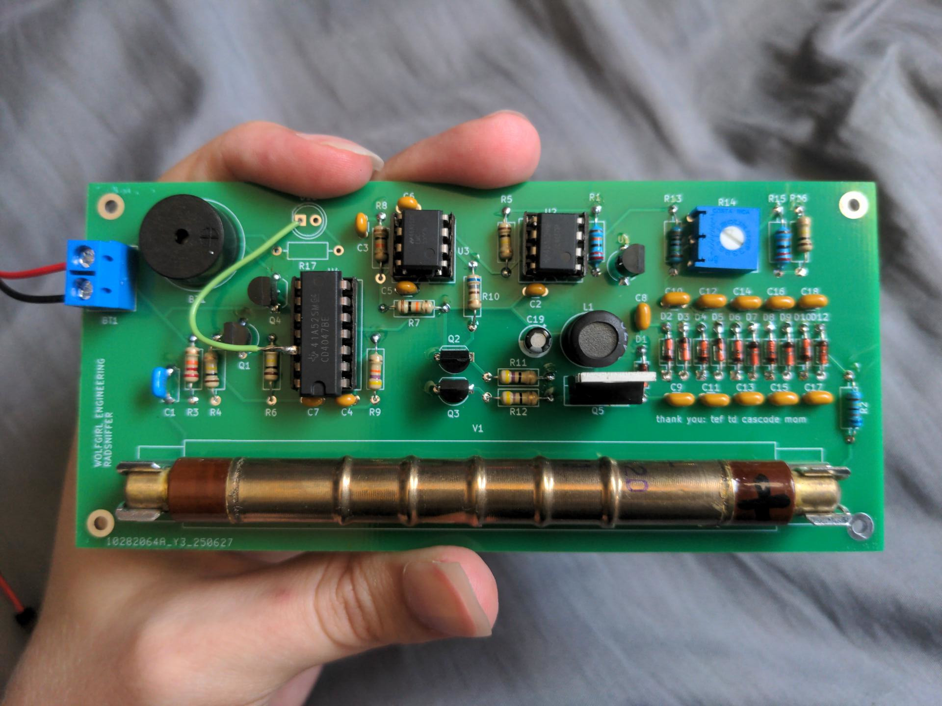
here it is!!
and it fricken' works. The PCB I had made is an earlier version with an issue that caused the buzzer to go forever (somewhere in the process I made a change that made it necessary to pull the 4047s RETRIGGER pin to ground). But after adding a jumper to fix it, it works. Oh she works and I am so proud…
There is a lot that I want to do differently if I do something like this again. I am better at making footprints now. The silkscreen of my tube footprint is inaccurately large and a little bit silly. The board edges could have a nice fillet. My very nicely intact ground plane on the bottom layer is wasted by my one PWM trace getting jumped right over a power trace via R10 anyways. Its a mess, but it was a long project, and I learned a lot.
kicad project file on sourcehut
finished july 8th, 2025